ECE Assistant Professor Farimah Farahmandi has received funding from the Office of Naval Research (ONR) in support of her three-year project, “SVH: Security Verification of Heterogenous Integration.” The $510k grant supports work which aims to develop novel security verification techniques to check against integration and lifecycle threats that impact the confidentiality, integrity, and availability of heterogenously integrated devices, commonly known as ‘Systems-in-Package’ (SiP).
HETEROGENOUS INTEGRATION
What is heterogeneous integration (HI)? The terms refers to the integration of separately manufactured components into a higher-level assembly—a system-in-package (SiP)—that in the aggregate provides enhanced functionality and improved operating characteristics. In this context, a component can be taken to mean any unit, such as a microelectromechanical system, assembled package for high-bandwidth memory—such as passive components—and others.
[ ee times ]
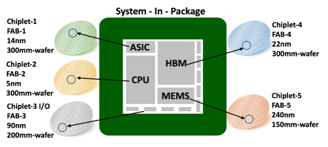
 HI (as shown in the illustration) allows separately fabricated components such as chiplets (custom-made silicon die for a specific application) to work together to form a higher-level assembly, the SiP.
The move towards HI is primarily driven by three factors. First, technological diversity – various chiplets with different technology nodes and foundries can be integrated on the same package using an intermediate silicon layer called interposer. Second, functional diversity – individual components such as chiplets (memory, logic, or I/O) or MEMS sensors can be integrated into a single package. Third, materials diversity – newer materials can be used to optimize the chiplet for a specific function and capabilities.
SECURITY VERIFICATION
With the increased complexities of SiPs, conventional pre- and post-silicon verification techniques can’t be applied to fabricated chiplets, making SiP security verification quite challenging and unique. To address these concerns, the work outlined in the NSF project will pursue two parallel approaches: static security verification and runtime security property monitoring.
Static Security Verification
Utilizing the system specification (usually provided by the customer or design house), the team will develop security policies/properties to ensure confidentiality, integrity, and availability requirements for targeting security-critical assets and to provide mitigation strategies if any of the policies are violated.
Runtime Security Property Monitoring
A promising solution would be to add at-speed security monitoring capabilities to the package itself, thereby enabling runtime security policy/property checking and enforcement. Runtime security policy can be done using an innovative integrated chiplet hardware security module (CHSM), implemented using an embedded FPGA fabric. Using existing tools, these CHSMs are embedded as additional modules in chiplets. The CHSM can subsequently be updated to respond to unknown and zero-day attacks. This innovative approach is believed to be the first-ever comprehensive security verification technique specifically for SiPs. The hope is that this new method will prove to be capable of identifying and mitigating vulnerabilities during pre- and post-silicon, as well as at runtime.