Categories
News

Korea moves closer to becoming global semiconductor hub

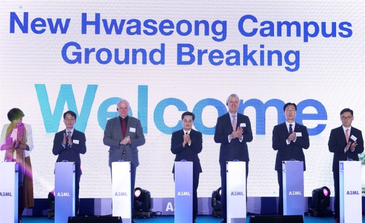
Korea is moving to become a hub for the semiconductor industry, as global chip companies are building their facilities here one after another. As part of its efforts, ASML, the Netherlands-based semiconductor equipment maker, held a groundbreaking ceremony to build its facility in Hwaseong, Gyeonggi Province, Wednesday.

Categories
News

Physical Assurance & Inspection Videos Hit 100k Milestone

ECE Assistant Professor (and budding social media star) Navid Asadi’s 12-part video series, ‘Physical Assurance and Inspection of Electronics,’ recently surpassed 100k views.

Categories
News

How using analytics and AI can help companies manage the semiconductor supply chain

By crunching through the massive amounts of data being generated by today’s supply chains, AI can predict a range of unexpected events, such as weather conductions, transportation bottlenecks, and labor strikes, helping to anticipate problems and reroute shipments around them.

Categories
News

Legacy Tools, New Tricks: Optical 3D Inspection

White light interferometry and other optical approaches can help detect defects in advanced packages. Stacking chips is making it far more difficult to find existing and latent defects, and to check for things like for things like die shift, leftover particles from other processes, co-planarity of bumps, and adhesion of different materials such as dielectrics.

Categories
News

Chip Sustainability Efforts Get Their Own Consortium

Going green is becoming table stakes no matter the sector, and the semiconductor industry formalized a commitment to sustainability by launching the Semiconductor Climate Consortium (SCC).

Categories
News

Fan-Out Packaging Gets Competitive

Fan-out wafer-level packaging (FOWLP) is a key enabler in the industry shift from transistor scaling to system scaling and integration. The design fans out the chip interconnects through a redistribution layer instead of a substrate. Compared to flip-chip ball grid array (FCBGA) or wire bonds, it creates lower thermal resistance, a slimmer package, and potentially lower costs.

Categories
News

3D-STACKED CMOS TAKES MOORE’S LAW TO NEW HEIGHTS

When transistors can’t get any smaller, the only direction is up.

Categories
News

Finding Talent to Run New Fabs Might Be Challenging

The U.S. CHIPS and Science Act spurred a rush to build new semiconductor fabs in the United States. So far, there are at least nine new fabs planned or under construction, as well as expansion plans at many existing fabs. One challenge the industry faces is matching a huge influx of fab capacity worldwide with the notorious boom-bust cycles of the semiconductor industry. But there may be another challenge looming: having enough skilled labor to operate and support these fabs.

Categories
News

Pushing the Power of Heterogeneous Integration

ECE Assistant Professor Farimah Farahmandi has received funding from the Office of Naval Research (ONR) in support of her three-year project, “SVH: Security Verification of Heterogenous Integration.” The $510k grant supports work which aims to develop novel security verification techniques to check against integration and lifecycle threats that impact the confidentiality, integrity, and availability of heterogenously integrated devices, commonly known as ‘Systems-in-Package’ (SiP).

Categories
News

Leading the Way in Physical Assurance

ECE Assistant Professor Navid Asadi reminds us of another issue with modern chips—physical assurance. Put another way, how can we be sure that the chips inside our devices are safe, reliable, and will perform as they were designed? As the bulk of chips are fabricated outside the purview of the U.S., these questions are even more critical in a national security sense.